Before the iron
The pack is about 18 to 21 volts. A strand from B+ to B- welds and can start a fire. Unplug the USB lead. Take the shoe off the pack. Solder on the bare boards.
The yellow jumper on the blue board stays on 3V3. The 5V pad is not used.
Gold is the only new lead that may touch B+. It runs from HV on the red board to the outer blade. It never lands on the FT232. The yellow wire already in the plug is TXD, not B+.
Hold J2 low before the shoe touches the pack. If J2 sits high while you plug in, the pack counts a dumb charge. Run the idle step in the public reader first, then seat the shoe, B- first.
Your parts
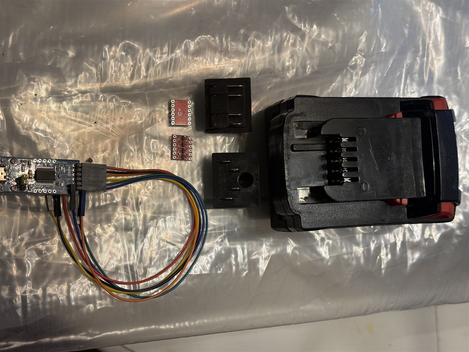
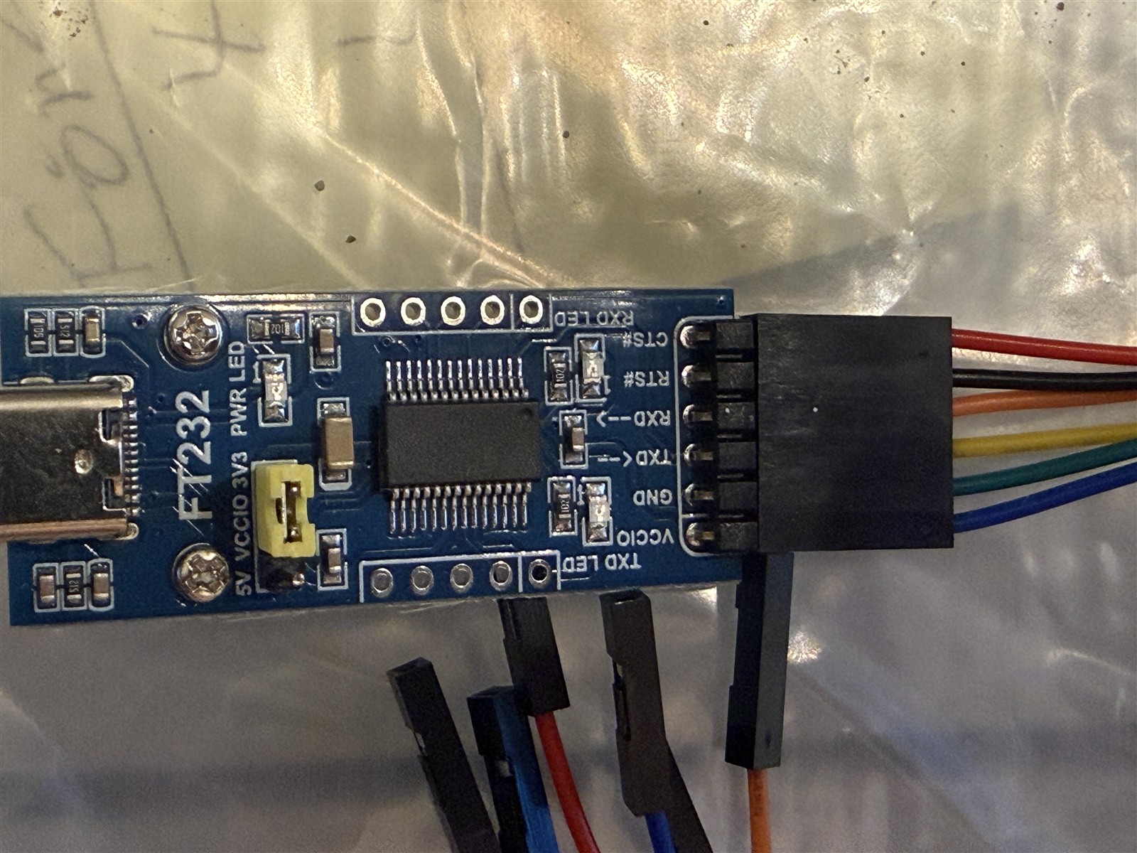
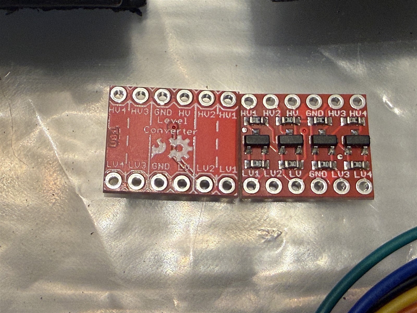
The cords
These are the six wires already in the grey shell, top to bottom, plus one new gold wire.
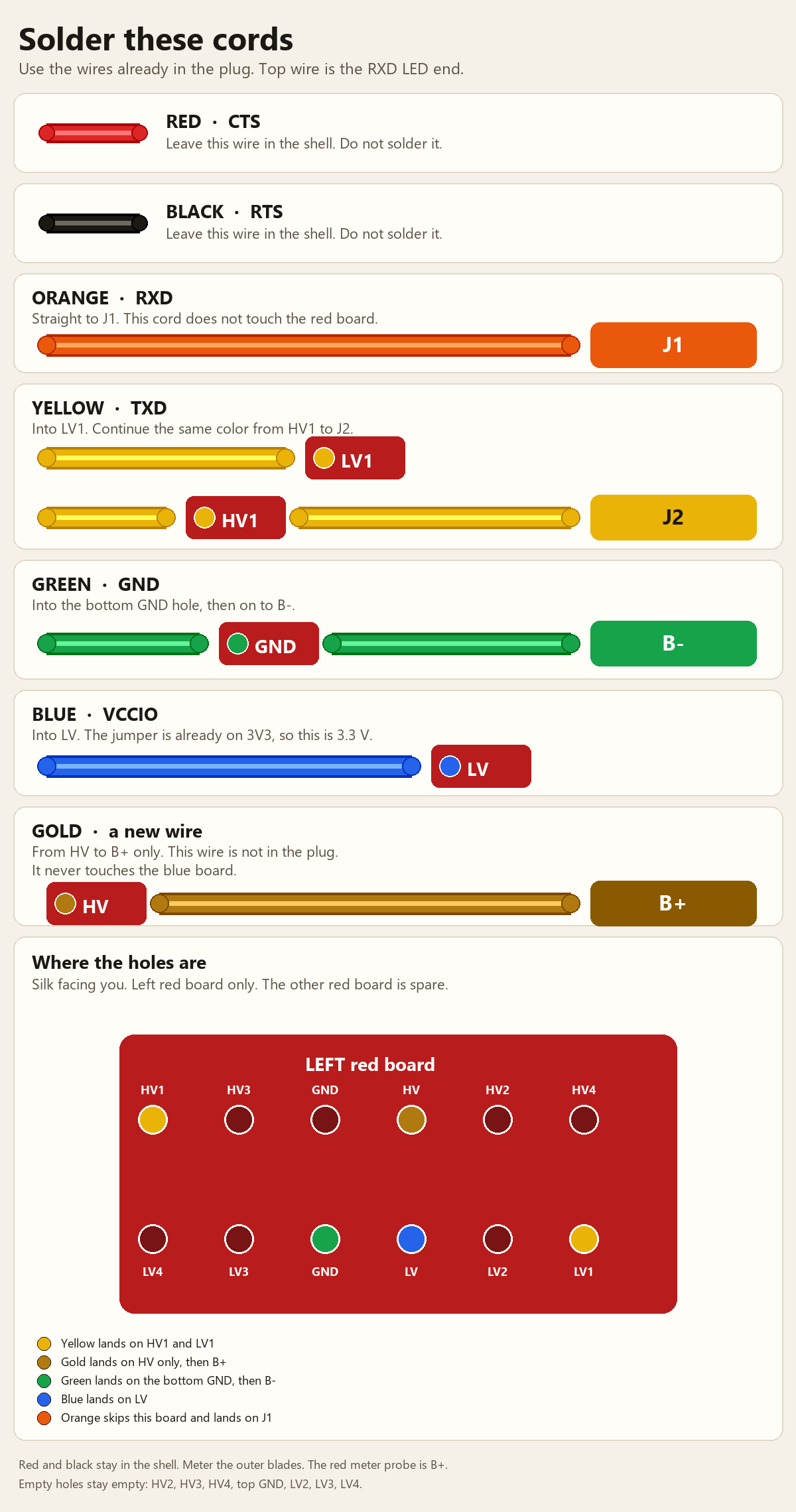
| Cord in the plug | Silk on the blue board | Solder it to |
|---|---|---|
| Red, top wire | CTS | Nowhere. Leave it in the shell. |
| Black | RTS | Nowhere. Leave it in the shell. |
| Orange | RXD | Pack blade J1. This cord does not touch the red board. |
| Yellow | TXD | Red board LV1, the bottom-right hole. Continue yellow from HV1, the top-left hole, to pack blade J2. |
| Green | GND | Red board bottom GND, and on to pack blade B-. |
| Blue | VCCIO | Red board LV. The jumper is on 3V3, so this pad is 3.3 V. |
| Gold, new wire | Not on the blue board | Red board HV to pack blade B+. Nowhere on the FT232. |
Leave empty: the 5V pad, HV2, HV3, HV4, the top GND, LV2, LV3, LV4, the second red board, and the square black block. If a pad says DTR, leave it open. Bridge DTR to TXD on the adapter only if the pack never answers. That bridge is for clone chips that cannot hold a break.
Which blade is which
The two outer blades are power. The two inner blades are the data pair. Do not trust left and right from a photo of a pack that can be turned around.
- Meter the two outer blades on DC volts. You should read about 18 V. The red meter probe is on B+.
- J1 is the inner blade touching B+. J2 is the inner blade touching B-.
- Put tape on the B+ end of the long black shoe before you solder, so it cannot be flipped later.
- The inner blades are not the 18 V pair. If the meter reads pack voltage on an inner blade, stop and look again.
Solder order
- USB unplugged. Shoe off the pack. Jumper still on 3V3. Red and black wires stay in the shell.
- Green from the plug GND pad to the red board’s bottom GND hole, then on to the shoe pin you marked B-.
- Blue from VCCIO to LV.
- Yellow from TXD to LV1. A second yellow from HV1, the top-left hole, to the shoe pin for J2.
- Orange from RXD straight to the shoe pin for J1.
- New gold wire from HV to the shoe pin you marked B+. Check that gold never touches a pad on the blue board.
- Look for a solder bridge between B+ and any other pin. Wick it before power.
- Plug USB. Run idle in the public reader so J2 is held low. Then seat the shoe, B- first.
Voltage check
Meter from B- to each data blade, after the shoe is seated.
| J2, next to B- | J1, next to B+ | |
|---|---|---|
| Idle | under 1 V | under 1 V |
| High | over 8 V | over 2 V |
A healthy pair on the published bench was about 0.13 V and 0.81 V at idle, and about 8.8 V and 3.3 V when high. If the red board gets hot, unplug. If J1 stays over 1 V at idle, this kit does not include the two-transistor isolator. Stop there.
The same four blades are on every M18 shell: CP, XC, High Output, HD, and Forge. Amp-hours change the cells inside the shell. They do not move these four contacts.
Source
The pad names follow the public wiring drawing and the device notes in discussion 16. The cord colors are the ones already in this plug. This page does not ship that software.
Wiring drawing and device list: